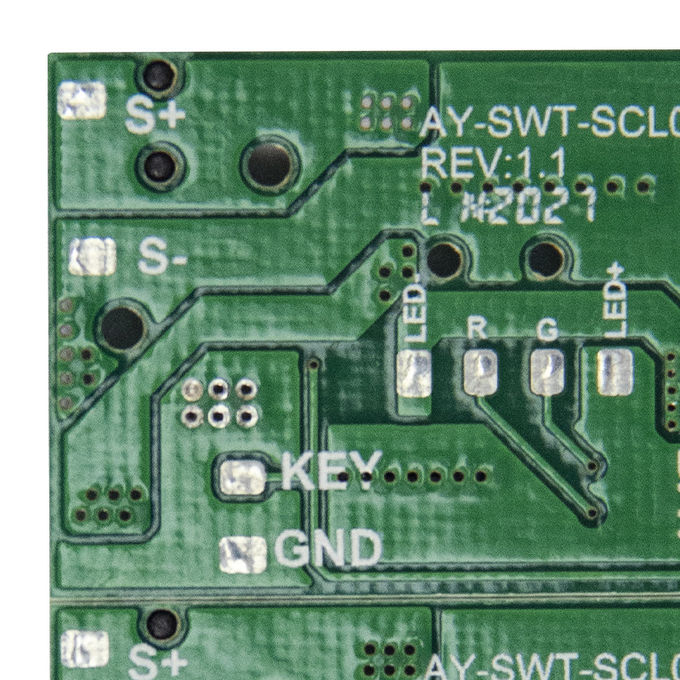
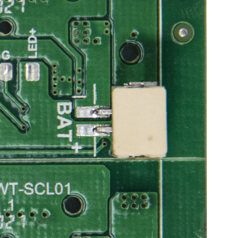
Insert one end of the PCB board into the connector card slot, use the connector pin as the outlet of the pcb board to connect to the outside, so that the pad or copper skin contacts the pin at the corresponding position to achieve the purpose of conduction, and the pcb board This pad or copper is coated with gold or nickel-gold, which is called a gold finger because it is shaped like a finger.
| Sign In | Join Free | My carsrow.com |
|
- Home
- Products
- About Us
- Quality Control
- Contact Us
- Get Quotations


